{
“title”: “Navigating EMI Filters and Noise Mitigation in EV Power Electronics for Robust EMC Compliance”,
“content”: “
Ensuring compliance with both safety and ElectroMagnetic Compatibility (EMC) regulations is a critical, yet often challenging, aspect of designing power electronics for electric vehicles (EVs). While safety standards are generally well-understood by engineers, navigating the intricacies of EMC compliance can present a steeper learning curve. However, a solid grasp of fundamental physics and strategic design choices can significantly mitigate these challenges.

nn
Understanding the Fundamentals of EMC Compliance
nn
EMC regulations fundamentally aim to achieve four key objectives: minimizing the emission of electromagnetic interference (EMI) and maximizing immunity to it, across both conducted and radiated pathways, within a specified frequency range. This typically spans from 150 kHz to 2.5 GHz.

nn
At higher frequencies, electromagnetic radiation becomes the primary route for EMI to enter or leave a device. This is because wiring lengths and enclosure openings can approach half a wavelength (where wavelength, λ, in meters = 300 / f in MHz), effectively transforming them into efficient antennas. Conversely, at lower frequencies, the attenuation caused by parasitic inductances and capacitances in wiring and PCB traces increases, making conducted EMI the dominant concern.
nn
While there isn’t a strict frequency dividing line, most EMC testing standards focus on conducted noise below 30 MHz and radiated noise above it. Given that formal EMC compliance testing can incur substantial costs, often in the thousands of dollars per hour, proactively identifying and resolving noise issues during the design phase is economically prudent.
nn
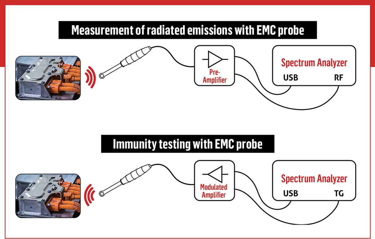
Leveraging Diagnostic Tools for Early Detection
nn
A significant amount of noise troubleshooting can be performed cost-effectively using a set of near-field EMC probes and a spectrum analyzer, ideally equipped with a tracking generator. These tools offer advantages over the antenna-based setups used in formal testing, particularly for pinpointing radiated emissions and immunity problems.
nn
Near-field probes can distinguish between RF currents (H-field) and voltages (E-field), providing granular insights into the source of interference. For immunity testing, H-field probes can be driven by an external RF source, such as a spectrum analyzer’s tracking generator, to expose circuit traces, wiring, and enclosure openings to high field strengths with minimal power. This contrasts with far-field testing, which requires significantly more power.
nn
Evaluating conducted emissions and immunity necessitates a specialized filter known as a Line Impedance Stabilization Network (LISN). This device decouples the power supply from the Device Under Test (DUT). While LISNs can be self-constructed, commercially available options offer a cost-effective solution.
nn
Conducted emissions are measured using a spectrum analyzer by passing power or signal wires through a wideband current transformer calibrated for EMC testing. Conducted immunity, on the other hand, is assessed through Bulk Current Injection (BCI), where RF current is injected into wires connected to the DUT via an inductive coupler.
nn
Addressing Common Mode and Differential Mode Noise
nn
The majority of noise issues stem from common-mode voltages or currents—those with similar amplitude and phase across multiple wires. Differential-mode noise can also be addressed by altering the direction of the forward or return wire through the current transformer or BCI device, respectively. This adjustment should ideally reduce the measured or injected value by 3 dB.
nn
For those seeking deeper knowledge, comprehensive resources include Kenneth Wyatt’s three-part book series on EMC and Tim Williams’ “EMC for Product Designers.” Additionally, YouTube channels hosted by Hans Rosenberg and Dr. EMC offer valuable insights.
nn
Proactive Design Strategies for EMC Excellence
nn
Preventing EMC issues through thoughtful design is far more effective than rectifying them later. A key high-level design decision involves adopting soft-switching (quasi-resonant) or fully resonant converter topologies. Although these can be more complex to implement, they typically exhibit reduced switching transition ringing—a common cause of EMC test failures—and often offer superior efficiency.
nn
Board-Level Design Principles
nn
On the printed circuit board (PCB) level, implementing a solid ground or return plane as one of the inner layers is a highly effective strategy. A solid ground plane, positioned close to signal and power traces, effectively cancels out nearly all radiating H-fields, thereby reducing both noise emissions and susceptibility. It also has the beneficial effect of lowering trace inductance.
nn
A crucial corollary to this principle is to avoid splitting or interrupting the ground plane, except where galvanic isolation is strictly necessary. While older advice sometimes suggested splitting ground planes between noisy and quiet circuits, using a single, large ground plane for all components (unless galvanic isolation is required) is generally preferable. This avoids the risk of high-frequency currents traversing unintended paths.
nn
For galvanically isolated ground planes, a common-mode current return path can be established using Y-capacitors (rated for line-to-earth use) that connect back to the main, earthed ground plane. These capacitors help quiet the isolated plane.
nn
Furthermore, employing termination techniques for high-speed digital signal traces or wires is essential. This can involve a series resistor at the source or “split termination” at the receiver. Many modern components, such as FPGAs and DSPs, offer built-in pin-level termination options. It is also vital to be cautious about capacitively coupling high dV/dt signals from high-voltage, high-frequency switches (like GaN HEMTs) to the external environment, as this can inadvertently turn enclosures into significant EMI radiators.
nn
Wiring and Interconnect Best Practices
nn
Inside devices featuring high-power switchmode converters—common in EV systems—all board-to-board interconnects should utilize differential signaling or pair each single-ended signal wire with a dedicated return wire. Ribbon cables, especially those with twisted-pair construction, facilitate these configurations and help minimize EMC issues. Differential signaling provides the maximum benefit with twisted-pair wiring.
nn
While cable shielding can be effective against EMI, it can also become a source of interference if improperly implemented. Key guidelines include treating the shield as part of the enclosure rather than a high-frequency current return path, and ensuring the shield is bonded circumferentially at enclosure ends, avoiding soldered pigtails.
nn
A common solution for wiring EMC problems is the use of clip-on or molded common-mode chokes (CMCs). These chokes, made from lossy ferrite materials, are most effective on low-impedance wires and cables, particularly when emissions are the primary concern. CMCs should be placed at the ends of cables, as antenna impedance is lowest there at half-wavelength resonances.
nn
AC or DC power inputs and DC outputs typically require some form of common-mode filtering. AC mains filters, in particular, must meet safety agency certifications, making off-the-shelf products the most practical choice.
nn
Enclosure Design and Shielding for EMI Control
nn
Slots, holes, and poorly bonded seams in device enclosures are frequent and often unavoidable sources of EMC problems. Rectangular openings and imperfect seams act as more efficient antennas than round holes. A general rule of thumb is to keep the longest dimension of any opening below λ/20 of the highest relevant frequency, with λ/50 being ideal.
nn
For instance, if the highest frequency of concern is 25 MHz, an opening should not exceed approximately 24 cm. However, if dealing with 2.4 GHz signals, the maximum permissible opening shrinks to a mere 6.25 mm, highlighting the frequency-dependent nature of these rules.
nn
Poorly bonded seams, especially common with aluminum due to its oxide layer, can also compromise EMC performance. This issue can be exacerbated by anodizing, paint, powder coating, or insufficient fasteners. Effective, though costly, solutions include metal mesh gaskets. Nickel plating aluminum can ensure good contact even with fewer fasteners.
nn
Metal shielding, while often labor-intensive and costly, can be an indispensable last resort. It is particularly relevant for components like LCD displays, which often necessitate openings that can lead to excessive EMI leakage. If relocating the display is not feasible, a metal shield may be the only viable solution.
nn
Even thin, highly conductive metal shielding effectively blocks high-frequency E- and EM-fields, provided it is solidly bonded to ground to minimize inductance. For H-fields, shielding relies on material permeability at low frequencies and eddy current induction at higher frequencies. The effectiveness of shielding is directly proportional to its thickness.
nn
Similar to traces and wiring, shielding requires solid bonding to the enclosure or ground plane to provide a return path for induced noise currents. Failure to do so can transform the shield into an unintended antenna. For magnetic components like E-core transformers, confining the magnetic gap to the center post and using a “flux band”—a single wrap of copper foil around the coil former and legs—can effectively contain stray magnetic fields. Crucially, any such shield must be properly bonded to the ground plane to prevent it from becoming a radiator itself.
”
}