Key Takeaways (TL;DR)
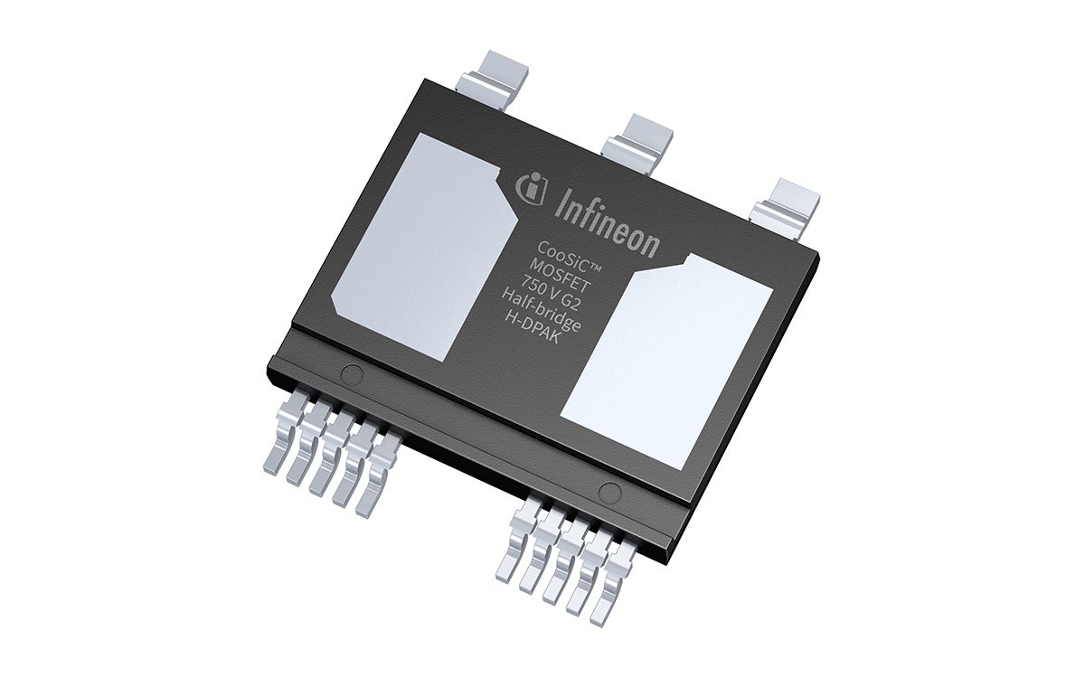
- Infineon has launched the H-DPAK, an innovative semiconductor package housing a complete 750 V CoolSiC G2 silicon carbide (SiC) half-bridge.
- This integrated solution streamlines power conversion designs for electric vehicle (EV) on-board chargers (OBCs), DC-DC converters, and other high-power automotive and industrial applications.
- The H-DPAK features a top-side cooled design and a unique split lead frame, significantly enhancing thermal performance and reducing parasitic inductance for improved efficiency and reliability.
- Its board-level compatibility and compact 2.3 mm height offer a drop-in solution for existing layouts, accelerating design cycles for engineers.
- The CoolSiC G2 technology within provides low gate charge, high dv/dt capability, and wide gate-bias tolerance, optimising performance in demanding power electronics systems.
Infineon Technologies, a global leader in power semiconductors, has unveiled a significant advancement in power conversion technology with the introduction of its H-DPAK package. This innovative solution integrates a complete 750 V CoolSiC G2 silicon carbide (SiC) half-bridge within a single, top-side-cooled package, poised to transform the design landscape for electric vehicle (EV) power electronics and various industrial systems.

The new H-DPAK is specifically engineered to address the growing demands for higher efficiency, greater power density, and enhanced reliability in critical applications such as single-stage and two-stage on-board chargers (OBCs), DC-DC converters, and EV auxiliaries. Beyond automotive, its capabilities extend to high-voltage direct current (HVDC) AI server power supplies and essential battery backup units, underlining its versatility and impact across diverse high-power sectors.
The Strategic Shift to Integrated Half-Bridge Solutions
Historically, power conversion designs often relied on mounting discrete high-side and low-side switches separately on a printed circuit board (PCB). This approach, while functional, presented challenges related to space utilisation, interconnection complexities, and managing parasitic elements that can hinder performance, especially at high switching frequencies.
The H-DPAK fundamentally redefines this paradigm by consolidating the entire unidirectional half-bridge into a single, compact package. This integration not only reduces the physical footprint required on the PCB but also optimises the electrical path between the switches, paving the way for more efficient and robust power stages.

An integrated half-bridge simplifies the layout and assembly process for engineers. By providing a pre-optimised power stage within one component, it eliminates the complexities associated with matching and positioning discrete devices, thereby reducing design time and potential errors.
Engineering for Optimal Performance: Package Design Innovations
Infineon’s H-DPAK package is a testament to sophisticated engineering, incorporating several design features aimed at maximising performance and reliability in demanding environments. These innovations are critical for unlocking the full potential of SiC technology in real-world applications.
Advanced Thermal Management through Top-Side Cooling
Effective thermal management is paramount for power semiconductors, particularly in high-power density applications like EV on-board chargers. The H-DPAK’s top-side cooling orientation is a key differentiator, enabling seamless integration with liquid cooling systems in densely packed power stages. This design choice eliminates the need for extensive board redesigns, offering a more direct and efficient heat dissipation path.
Traditional bottom-side cooled packages often require heat to travel through the PCB to a heatsink, which can be less efficient and limit the achievable power density. With top-side cooling, heat is drawn directly away from the power device, allowing for superior thermal performance and the operation of components at higher power levels without compromising reliability or lifespan.
The integration capabilities of top-side cooling are particularly beneficial for modern EV architectures where space is at a premium and thermal performance directly impacts system efficiency and longevity. This approach ensures consistent and reliable operation even under extreme thermal loads.
Mitigating Parasitic Effects with Split Lead Frame Design
The H-DPAK features a unique split lead frame design with optimised drain pads. This meticulous engineering plays a crucial role in improving heat spreading from the device, further enhancing its thermal capabilities. More importantly, it significantly reduces parasitic loop inductance within the power stage.
Parasitic inductance is an inherent challenge in high-frequency switching applications. In SiC devices, known for their rapid switching speeds (high dv/dt rates), unchecked parasitic inductance can lead to increased switching losses, voltage overshoots, and electromagnetic interference (EMI). By minimising this inductance, the H-DPAK effectively reduces switching noise and ringing, ensuring cleaner and more stable power conversion.
This reduction in unwanted electrical phenomena contributes to greater system efficiency, improved electromagnetic compatibility, and enhanced overall reliability. It allows designers to fully leverage the high dv/dt capabilities of SiC without encountering detrimental side effects, pushing the boundaries of power converter performance.
The Power of 750 V CoolSiC G2 Silicon Carbide Technology
At the heart of the H-DPAK lies Infineon’s advanced 750 V CoolSiC G2 silicon carbide MOSFET technology. SiC has emerged as a game-changer in power electronics due to its superior material properties compared to traditional silicon, offering higher breakdown voltage, faster switching speeds, and better thermal conductivity.
The 750 V CoolSiC G2 silicon further refines these advantages, bringing specific enhancements that directly translate to improved application performance. A key feature is its low gate charge, which is fundamental to reducing gate drive losses. Lower gate charge means less energy is required to switch the MOSFET on and off, directly contributing to higher overall system efficiency, especially at high switching frequencies.
Furthermore, the G2 technology boasts high dv/dt capability. This refers to the ability of the device to handle rapid changes in voltage over time, a characteristic essential for fast-switching SiC MOSFETs. High dv/dt capability ensures robust and efficient operation during transient conditions, which are common in demanding power conversion applications.
Finally, the wide gate-bias tolerance of the CoolSiC G2 silicon enhances the robustness and reliability of the device. This tolerance provides greater flexibility in gate drive design and ensures stable operation across varying conditions, safeguarding the system against potential operational instabilities.
Revolutionising EV Power Conversion: On-Board Chargers and DC-DC Converters
The Infineon H-DPAK is set to play a pivotal role in advancing electric vehicle power electronics, particularly in on-board chargers (OBCs) and DC-DC converters.
Optimising On-Board Chargers (OBCs)
OBCs are essential components in EVs, converting AC power from the grid into DC power to charge the vehicle’s high-voltage battery. The drive for faster charging times, higher power output, and reduced size necessitates highly efficient and compact power conversion solutions.
The H-DPAK, with its integrated half-bridge and superior thermal management, is ideally suited for both single-stage and two-stage OBC architectures. Its ability to manage heat effectively allows for higher power density, meaning more power can be delivered in a smaller volume, crucial for space-constrained EV designs. The reduced switching losses from the CoolSiC G2 technology contribute directly to the overall efficiency of the charging process, minimising energy waste and heat generation.
Enhancing DC-DC Converters and EV Auxiliaries
DC-DC converters manage power flow between different voltage domains within an EV, such as stepping down the high voltage battery output to power the 12V auxiliary systems. Efficiency and reliability are paramount here to minimise losses and ensure consistent operation of critical vehicle functions.
The H-DPAK’s high efficiency and reduced parasitic effects make it an excellent choice for these converters, contributing to extended range and improved system longevity. Furthermore, its benefits extend to other EV auxiliaries, where efficient and compact power solutions are increasingly desired to reduce the overall weight and complexity of the vehicle’s electrical system.
Expanding Horizons: Industrial and Data Centre Applications
While a primary focus is on automotive applications, the H-DPAK’s advanced features also make it highly suitable for demanding industrial and data centre environments. The need for high-efficiency power conversion is universal across these sectors, driven by energy conservation targets and increasing computational power requirements.
HVDC AI server power supplies, for instance, demand robust and efficient power delivery to handle the immense energy consumption of modern artificial intelligence infrastructure. The H-DPAK’s capabilities in managing high voltages and switching rapidly with minimal losses are invaluable here, contributing to greener and more reliable data centres. Similarly, in battery backup units, where uninterrupted and efficient power conversion is critical, the H-DPAK offers a dependable solution that enhances system performance and reduces operational costs.
Seamless Integration for Accelerated Design Cycles
Infineon has meticulously designed the H-DPAK with board-level compatibility as a core consideration. Matching the compact 2.3 mm height of Infineon’s existing Q-DPAK and TOLT packages, the H-DPAK provides a convenient drop-in compatible option for layouts already established around these footprints. This thoughtful design choice significantly streamlines the integration process for manufacturers and speeds up the time-to-market for new products.
Engineers can leverage existing PCB designs, minimising the need for costly and time-consuming redesigns. This compatibility ensures that the benefits of the H-DPAK’s advanced SiC technology can be adopted with minimal disruption to current manufacturing processes, fostering innovation across the power electronics industry.
Infineon’s Strategic Vision for Power Semiconductors
The introduction of the H-DPAK underscores Infineon’s ongoing commitment to pushing the boundaries of power semiconductor technology. By offering highly integrated, efficient, and thermally optimised solutions, the company continues to solidify its position as a key enabler for the global transition towards sustainable mobility and energy-efficient industrial infrastructure. This latest innovation is a testament to the continuous evolution in power electronics, driven by the increasing demands of modern technological landscapes.
Frequently Asked Questions (FAQ)
What is the Infineon H-DPAK?
The Infineon H-DPAK is a new semiconductor package that integrates a complete 750 V CoolSiC G2 silicon carbide (SiC) half-bridge. It is designed to provide a compact, highly efficient, and robust solution for power conversion in automotive and industrial applications, streamlining design processes and enhancing performance.
What are the primary applications for the H-DPAK?
The H-DPAK is primarily designed for high-power conversion applications in electric vehicles, including single-stage and two-stage on-board chargers (OBCs), DC-DC converters, and EV auxiliaries. It also finds significant use in industrial systems such as HVDC AI server power supplies and battery backup units.
How does the H-DPAK improve thermal management?
The H-DPAK features a top-side cooling orientation, which allows for direct integration with liquid cooling systems in dense power stages without requiring board redesigns. Additionally, its split lead frame design with optimised drain pads further improves heat spreading, ensuring efficient thermal dissipation.
What are the benefits of the split lead frame design?
The split lead frame design with optimised drain pads not only enhances heat spreading but also significantly reduces parasitic loop inductance. This reduction minimises switching noise and ringing, which are common issues at the high dv/dt rates enabled by SiC technology, leading to more stable and efficient power conversion.
What is CoolSiC G2 SiC MOSFET technology?
CoolSiC G2 is Infineon’s second generation of 750 V silicon carbide (SiC) MOSFET technology. It offers superior performance compared to traditional silicon, featuring low gate charge for reduced gate drive losses, high dv/dt capability for fast switching, and wide gate-bias tolerance for enhanced robustness and reliability in power applications.
How does the H-DPAK simplify design for engineers?
The H-DPAK provides a complete integrated half-bridge in a single package, eliminating the need to mount discrete high-side and low-side switches separately. Its package geometry is designed for board-level compatibility, matching the 2.3 mm height of existing Q-DPAK and TOLT packages, offering a drop-in option that simplifies layouts and accelerates design cycles.
Why is SiC technology important for EV on-board chargers?
SiC technology is crucial for EV on-board chargers due to its ability to enable higher switching frequencies, higher power density, and superior efficiency compared to traditional silicon. This translates to faster charging times, smaller and lighter charger designs, and reduced energy losses during the charging process, all vital for modern EVs.
Does the H-DPAK offer advantages beyond automotive use?
Yes, beyond automotive applications, the H-DPAK’s high efficiency, robust thermal management, and compact design make it highly beneficial for industrial power supplies. This includes HVDC power supplies for AI servers, where energy efficiency is critical, and battery backup units, where reliable and high-performance power conversion is essential for uninterrupted operation.