
Key Takeaways
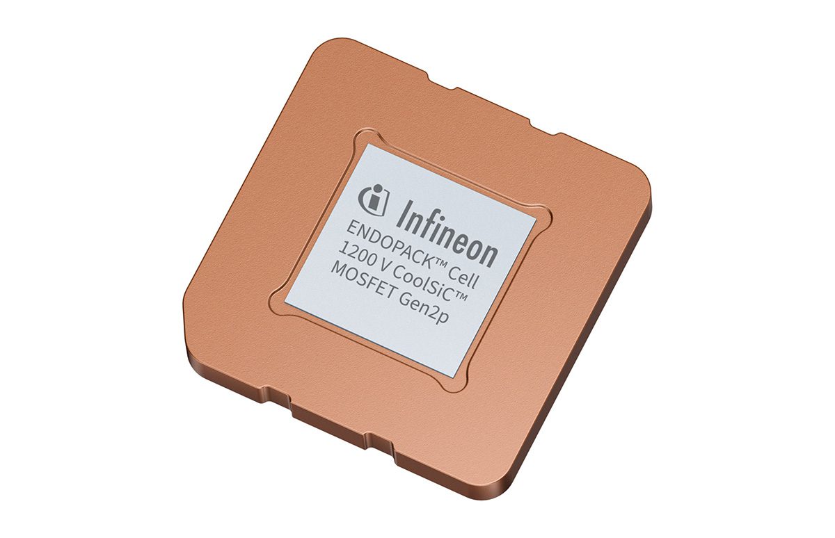
- Infineon has unveiled ENDOPACK Cell, a groundbreaking chip-embedding solution that integrates 1,200 V Automotive Gen2p CoolSiC MOSFETs directly into printed circuit boards (PCBs).
- This innovative approach is poised to accelerate the development of electric vehicle (EV) traction inverters and facilitate their seamless scaling across diverse vehicle platforms.
- ENDOPACK Cell leverages standardized PCB processes, potentially reducing development cycles by up to three times and offering a design-agnostic production pathway.
- The embedded architecture significantly lowers inductance to below 2 nH, leading to a 30% reduction in switching losses and achieving approximately 99.5% efficiency under CLTC conditions.
- Prototype data suggests the technology can boost power density to 200 kW/L and potentially enhance vehicle range by up to 7%.
- The solution allows for flexible configuration of power stages, adapting chip quantity and placement to specific vehicle performance and architecture demands, with mass production vehicles expected by 2027.
Infineon Technologies, a global leader in semiconductor solutions, has introduced a significant advancement in electric vehicle (EV) power electronics with its new ENDOPACK Cell. This innovative technology embeds high-performance 1,200 V Automotive Gen2p CoolSiC MOSFETs directly into a printed circuit board (PCB), marking a pivotal step towards more efficient and scalable traction inverter designs.
The introduction of ENDOPACK Cell is set to empower automotive manufacturers by significantly streamlining the development process for traction inverters. This integration capability allows for faster design iterations and greater flexibility, enabling automakers to deploy advanced power solutions across various vehicle platforms with unprecedented ease.

Pioneering Chip Embedding for High-Voltage EV Systems
ENDOPACK represents Infineon’s overarching brand for its advanced chip-embedding technologies. This family of solutions encompasses a wide array of voltage classes, form factors, and applications, demonstrating the company’s commitment to integrating semiconductors directly into system components.
While Infineon has successfully employed chip embedding in low-voltage production environments for some time, the expansion into high-voltage power electronics with ENDOPACK Cell signifies a major technological leap. This strategic move addresses the demanding requirements of modern EV drivetrains, where high voltage and extreme efficiency are paramount.
According to Infineon, ENDOPACK Cell stands out as the industry’s first automotive-qualified, high-voltage chip-embedding solution specifically engineered for direct PCB integration. This qualification underscores its robustness and reliability, meeting the stringent standards required for automotive applications.
Accelerated Development and Flexible Manufacturing
A core advantage of ENDOPACK Cell lies in its compatibility with established industry practices. The solution utilizes standardized PCB design processes and existing manufacturing infrastructure, removing potential barriers to adoption for automotive suppliers and manufacturers.
This standardization is projected to deliver substantial benefits in development timelines. Infineon estimates that ENDOPACK Cell can enable development cycles that are up to three times faster compared to conventional design approaches. Such a reduction in lead time is critical for the rapidly evolving EV market, allowing companies to bring new vehicle models to market more quickly.
Furthermore, ENDOPACK Cell is designed to seamlessly transfer to a ‘design-agnostic’ production line. This crucial feature means that design iterations can be implemented without necessitating repeated, costly, or time-consuming changes to the underlying manufacturing process. This flexibility empowers engineers to optimize designs iteratively, ensuring peak performance and efficiency without disrupting production workflows.
Unprecedented Efficiency and Power Density
The architectural innovation behind ENDOPACK Cell fundamentally redefines how power semiconductors are integrated. Instead of being mounted on top of a separate substrate, the power semiconductors are embedded directly within the PCB structure itself. This direct integration eliminates intermediate layers and connections, leading to profound electrical performance improvements.
One of the most significant benefits is a dramatic reduction in parasitic inductance. The ENDOPACK Cell architecture reduces inductance to below 2 nH, a substantial improvement when compared to typical conventional designs which can exhibit inductance levels around 20 nH. Lower inductance is vital in high-frequency switching applications like traction inverters, as it minimizes voltage overshoot and ringing, thus enhancing reliability and performance.
This reduction in inductance directly translates into a 30% decrease in switching losses. Switching losses, which occur every time a power semiconductor turns on or off, are a major contributor to inefficiency and heat generation in inverters. By mitigating these losses, ENDOPACK Cell significantly improves the overall energy conversion efficiency of the traction inverter, achieving approximately 99.5% efficiency under China Light-Duty Vehicle Test Cycle (CLTC) conditions.
Beyond efficiency, the embedded design also contributes to superior power density. According to prototype and simulation data provided by Infineon, ENDOPACK Cell can achieve peak power density of up to 200 kW per litre. This high power density is instrumental in allowing automakers to design more compact and lighter traction inverters, freeing up valuable space in the vehicle chassis and reducing overall vehicle weight.
Enhancing Vehicle Performance and Range
The collective improvements in efficiency and power density delivered by ENDOPACK Cell have direct positive implications for EV performance. The higher efficiency means less energy is wasted as heat, allowing more battery power to be converted into motive force. This optimized energy utilization can lead to a potential 7% improvement in vehicle range, according to Infineon’s data. For consumers, an extended range translates into greater driving convenience and reduced range anxiety.
Furthermore, the inherent flexibility of the ENDOPACK Cell architecture empowers engineers with unparalleled design freedom. The quantity and precise placement of the embedded chips can be readily adapted to meet specific power requirements and available installation space within a vehicle. This level of customization was previously constrained by the fixed geometry of conventional module housings.
The ability to integrate multiple ENDOPACK Cells into a single PCB further enhances this configurability. This modular approach allows the entire power stage of the traction inverter to be precisely configured to match the diverse performance demands and architectural specifics of any given vehicle platform. Whether it’s a compact urban EV or a high-performance sports utility vehicle, the solution offers tailored power delivery.
Roadmap to Mass Production
Infineon has confirmed that ENDOPACK Cell is not merely a concept but is ready for mass production. This readiness signals the company’s confidence in the maturity and scalability of the technology, assuring automakers of a stable supply chain for their future EV designs.
Looking ahead, vehicles incorporating Infineon’s ENDOPACK Cell technology are slated to enter mass production in 2027. This timeline positions ENDOPACK Cell to play a crucial role in the next generation of electric vehicles, contributing to advancements in efficiency, performance, and manufacturing agility across the global automotive industry.
As the electric vehicle market continues its rapid expansion, innovations like ENDOPACK Cell are vital in pushing the boundaries of what is possible in automotive power electronics. By offering faster development cycles, higher efficiency, and greater design flexibility, Infineon is setting a new benchmark for traction inverter technology.
Frequently Asked Questions (FAQ)
What is Infineon’s ENDOPACK Cell?
ENDOPACK Cell is Infineon’s new chip-embedding technology that integrates 1,200 V Automotive Gen2p CoolSiC MOSFETs directly into a printed circuit board (PCB). It aims to accelerate the development and scalability of traction inverters for electric vehicles (EVs).
How does ENDOPACK Cell improve EV traction inverter performance?
By embedding power semiconductors directly into the PCB, ENDOPACK Cell significantly reduces inductance to below 2 nH. This leads to 30% lower switching losses and an efficiency of approximately 99.5% under CLTC conditions, enhancing overall inverter performance.
What manufacturing advantages does ENDOPACK Cell offer to automakers?
The technology uses standardized PCB design processes and manufacturing infrastructure, allowing for development cycles up to three times faster. It also supports a design-agnostic production line, meaning design iterations can be made without repeated changes to the manufacturing process.
What are the key benefits for electric vehicle range and power density?
Prototype and simulation data indicate that ENDOPACK Cell can achieve a peak power density of up to 200 kW/L. This, combined with improved efficiency, can lead to a potential 7% improvement in overall vehicle range, offering better performance for EV users.
When can we expect vehicles using ENDOPACK Cell to enter mass production?
Infineon has stated that ENDOPACK Cell is ready for mass production, and vehicles incorporating this technology are planned to begin mass production in the year 2027.
Can ENDOPACK Cell designs be customized for different vehicle platforms?
Yes, the design allows for high flexibility. Chip quantity and placement can be adapted to specific power requirements and installation space, and multiple cells can be integrated into a single PCB to configure the power stage for a particular vehicle platform’s needs.