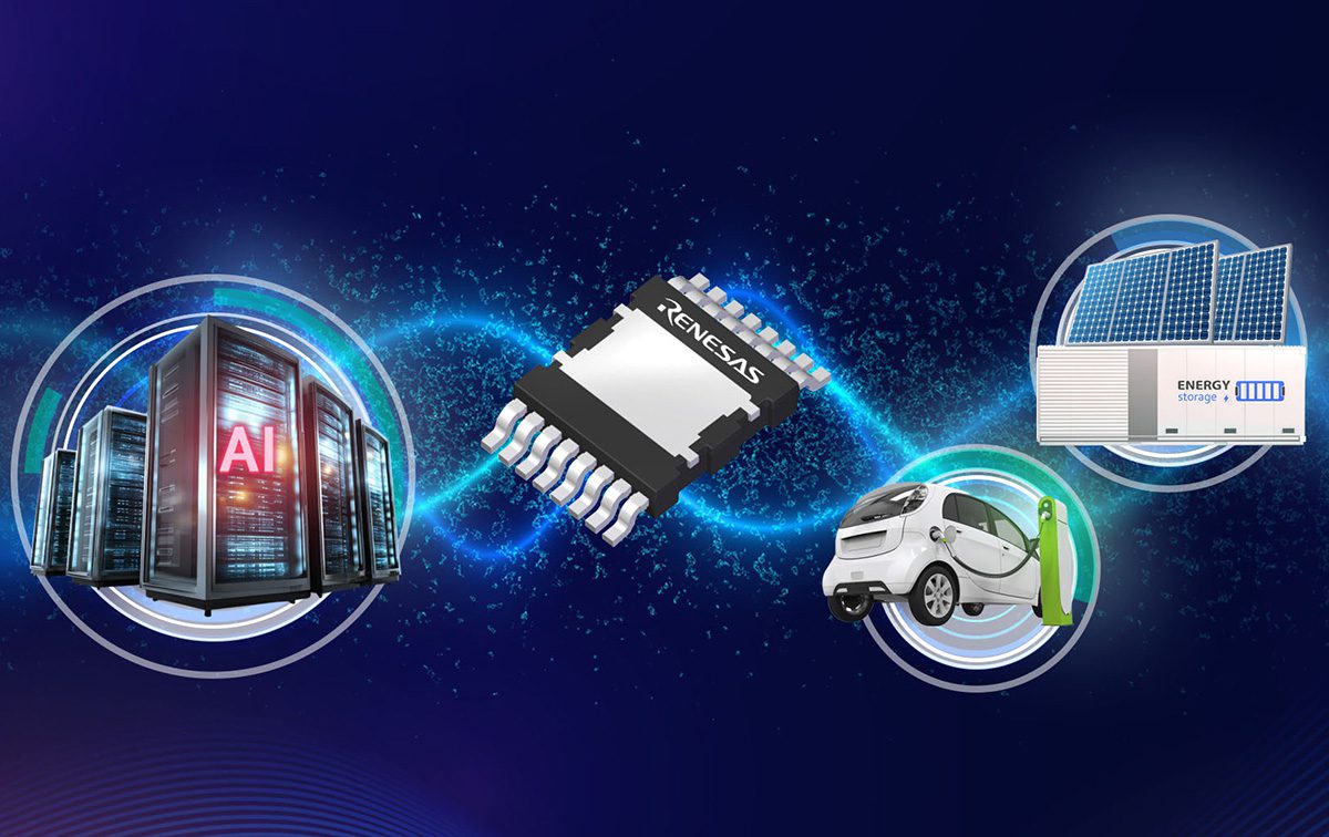
In a significant advancement for the semiconductor industry, Renesas has announced the introduction of what it describes as the industry’s first bidirectional 650 V-class Gallium Nitride (GaN) switch, complete with integrated DC blocking. This innovative component is poised to simplify complex power-conversion topologies across a range of high-demand applications, including solar microinverters, sophisticated AI data centers, and critical onboard EV chargers within the evolving landscape of EV power electronics.
The newly unveiled TP65B110HRU device marks a departure from conventional power management solutions. Its design allows it to block both positive and negative current within a single component, effectively eliminating the need for traditional arrangements that rely on multiple back-to-back Field-Effect Transistors (FETs). This integration promises to reduce component count, shrink device footprints, and enhance overall system reliability and efficiency.

Revolutionizing Power Conversion Topologies
The core innovation behind Renesas’s latest offering lies in its ability to streamline power conversion. In applications such as single-stage solar microinverters, the integration of just two of these new bidirectional SuperGaN devices can replace more intricate multi-stage configurations. This significantly reduces the total number of switches required and eliminates the need for intermediate DC-link capacitors, which are typically bulky and can be a point of failure.
Such a reduction in complexity and component count translates directly into palpable benefits for system designers and end-users. Fewer components mean lower bill-of-materials costs, reduced PCB area, and simplified design processes. Importantly, Renesas highlights real-world performance data, stating that a single-stage solar microinverter implementation leveraging this technology achieved an impressive efficiency exceeding 97.5%.
Technical Prowess: Integrated GaN and Silicon
At a technical level, the TP65B110HRU is a sophisticated co-packaged structure. It combines a high-voltage bidirectional depletion-mode GaN die with two low-voltage silicon MOSFETs. This hybrid approach leverages the superior switching characteristics of GaN while integrating silicon for specific functionalities, optimizing performance and integration.

The device is engineered to support continuous AC/DC operation across a robust ±650 V range and boasts a transient rating of ±800 V, making it suitable for demanding power environments. Its impressive specifications include a typical on-state resistance (RSS,ON) of 110 mΩ at 25 °C, a typical threshold voltage of 3 V, and a maximum Vgs of ±20 V. Furthermore, it exhibits dv/dt immunity above 100 V/ns, underscoring its robustness in fast-switching applications.
Packaged in a top-side-cooled TOLT format with an industry-standard pinout, the device is designed for ease of integration. A crucial design advantage is its compatibility with standard gate drivers, as it requires no negative gate drive. This simplifies driver circuit design and further accelerates adoption in various applications, particularly those focused on efficient EV power electronics.
Addressing Challenges in Enhancement-Mode GaN
Renesas emphasizes a major practical advantage that its new device holds over existing enhancement-mode bidirectional GaN devices. The latter often necessitate more complicated gate-drive schemes, which can add complexity and cost to power systems. By contrast, Renesas’s approach offers a straightforward solution without compromising performance.
Rohan Samsi, Vice President of Renesas’s GaN Business Division, articulated the direct benefits for customers, stating, “Customers can now achieve higher efficiency with fewer switching components, smaller PCB area and lower system cost.” This statement encapsulates the multifaceted advantages of the TP65B110HRU, pointing towards a new paradigm in power converter design across various sectors.
Implications for Key Industries
Advancements in Solar Microinverters
The solar energy sector is continually striving for greater efficiency, compactness, and reliability. Microinverters, which convert DC power from individual solar panels into AC power, are critical components. By reducing the number of power conversion stages and eliminating intermediate DC-link capacitors, Renesas’s new switch significantly contributes to creating more efficient, smaller, and more cost-effective microinverter designs. The reported 97.5% efficiency gain underscores its potential to boost energy harvesting from solar installations.
Boosting Efficiency in AI Data Centers
The exponential growth of Artificial Intelligence (AI) and machine learning necessitates increasingly powerful and energy-intensive data centers. Power conversion efficiency is paramount in these environments, where even marginal gains can lead to substantial reductions in operational costs and carbon footprint. The bidirectional 650 V GaN switch offers a pathway to more streamlined and efficient power supplies for AI accelerators and server racks. Its ability to simplify topologies can lead to denser power delivery units, saving valuable rack space and improving thermal management, vital considerations for high-performance computing infrastructure.
Enhancing Onboard EV Chargers and EV Power Electronics
The electric vehicle (EV) market is a prime beneficiary of advancements in power electronics. Onboard chargers, which convert grid AC power to DC power for the EV battery, must be compact, lightweight, and highly efficient. The TP65B110HRU’s capacity to reduce component count and simplify power conversion stages is particularly advantageous here. It enables manufacturers to design smaller, lighter, and more efficient onboard chargers, directly impacting vehicle range, charging speed, and overall EV performance. This innovation solidifies Renesas’s contribution to the evolving landscape of EV power electronics.
Beyond onboard chargers, the principles of efficient and compact power conversion extend to various other subsystems within an electric vehicle, including DC-DC converters and main inverters. As the demand for higher power density and extended range grows, advanced GaN devices like this become instrumental in pushing the boundaries of what is possible in EV power electronics design.
The Broader Impact of GaN Technology
Gallium Nitride (GaN) is increasingly recognized as a foundational material for the next generation of power electronics, offering distinct advantages over traditional silicon-based devices. GaN transistors can operate at much higher switching frequencies, withstand higher temperatures, and offer lower on-resistance, leading to significantly higher power efficiency and greater power density. This allows for smaller, lighter, and more cost-effective power solutions.
Renesas’s continuous investment in GaN technology, exemplified by this latest bidirectional switch, highlights the ongoing industry shift towards more advanced materials for critical power applications. The ability to integrate complex functionalities, such as bidirectional blocking, into a single GaN device represents a significant leap forward in the practical application of this material, particularly for demanding segments like EV power electronics.
Conclusion
The introduction of Renesas’s bidirectional 650 V GaN switch with integrated DC blocking is more than just a new product launch; it signifies a strategic step towards simplifying and enhancing power conversion across multiple high-growth sectors. By enabling higher efficiency, reduced component counts, and smaller form factors, the TP65B110HRU promises to unlock new possibilities in the design of solar microinverters, AI data center power supplies, and critically, the next generation of EV power electronics. This innovation reinforces Renesas’s position at the forefront of advanced power semiconductor development, offering solutions that meet the evolving demands for efficiency and compactness in a power-hungry world.