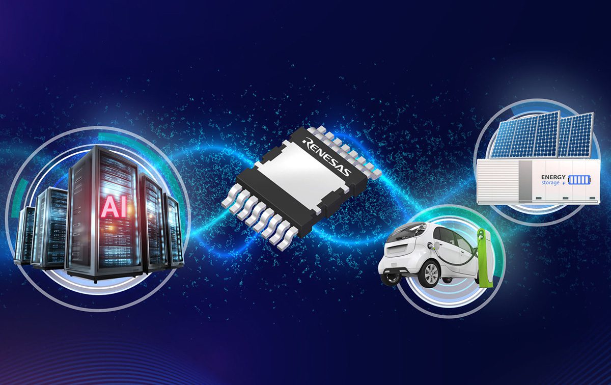
In a significant development for high-efficiency power conversion, Renesas has introduced what it describes as the industry’s first bidirectional 650 V-class Gallium Nitride (GaN) switch with integrated DC blocking. This innovative device, designed to simplify power-conversion topologies, holds substantial implications for a range of critical applications, including solar microinverters, advanced AI data centers, and crucial onboard EV chargers.
The new TP65B110HRU device marks a notable departure from conventional designs, which typically rely on cumbersome back-to-back FET arrangements. By uniquely integrating the capability to block both positive and negative current within a single component, Renesas aims to streamline system designs and enhance overall performance.

Rethinking Power Conversion Architectures
The core innovation of the TP65B110HRU lies in its ability to simplify complex power conversion stages. Traditional approaches often necessitate multiple discrete components and intricate circuitry to manage bidirectional current flow and DC blocking, increasing both component count and system complexity.
Renesas highlights a compelling example within single-stage solar microinverters. Here, just two of the new bidirectional SuperGaN devices can effectively replace more intricate multi-stage configurations. This reduction in component count leads to halving the number of switches required and eliminates the need for intermediate DC-link capacitors, critical for enhancing efficiency and reducing system footprint.
The practical benefits of this simplification are evident in real-world applications. The company reported that a single-stage solar microinverter implementation utilizing this new technology achieved an impressive efficiency exceeding 97.5%. Such gains are paramount for renewable energy systems, where every fraction of a percent in efficiency contributes to greater energy yield and reduced operational costs.

Technical Prowess and Integrated Design
From a technical standpoint, the TP65B110HRU is an advanced, co-packaged structure. It ingeniously combines a high-voltage bidirectional depletion-mode GaN die with two low-voltage silicon MOSFETs. This hybrid approach leverages the strengths of both material technologies to deliver robust and efficient performance.
The device is engineered to support continuous AC/DC operation across a wide range of ±650 V, with a transient rating extending to ±800 V. Its electrical characteristics further underscore its high performance: a typical RSS,ON of 110 mΩ at 25 °C ensures minimal power loss, while a typical threshold voltage of 3 V offers stable operation.
Furthermore, the switch boasts a maximum Vgs of ±20 V and dv/dt immunity exceeding 100 V/ns. These specifications are crucial for reliable performance in demanding power electronics environments, where rapid voltage changes and high switching frequencies are common.
Enhanced Integration and System Compatibility
Beyond its internal architecture, the physical design and interface of the TP65B110HRU have been optimized for ease of integration. It is housed in a top-side-cooled TOLT package, designed for efficient thermal management in compact applications.
Crucially, the device features an industry-standard pinout, ensuring compatibility with existing design ecosystems. A significant advantage highlighted by Renesas is that the device requires no negative gate drive, a common complexity associated with some power switches. This simplifies the gate driver circuitry, making it compatible with standard gate drivers and accelerating design cycles for engineers.
This design choice provides a major practical advantage, particularly when compared to enhancement-mode bidirectional GaN devices, which often necessitate more complicated gate-drive schemes. Such simplification reduces bill-of-materials, shortens development time, and enhances system reliability.
Driving Innovation in EV Power Electronics and Beyond
The introduction of this bidirectional GaN switch is poised to make a substantial impact across its target applications, particularly in the rapidly evolving field of EV Power Electronics. For onboard EV chargers, the ability to achieve higher efficiency with fewer components directly translates to smaller, lighter, and more powerful charging solutions, a critical factor for vehicle manufacturers striving to extend range and reduce vehicle weight.
In the context of AI data centers, where energy consumption and thermal management are constant challenges, the enhanced efficiency and reduced component count offered by the TP65B110HRU can lead to more compact and energy-efficient power supplies. This enables denser server racks and lower operational expenditures, crucial for the escalating demands of artificial intelligence workloads.
Solar microinverters, vital for distributed renewable energy generation, will benefit immensely from the simplified topologies and improved efficiency. This innovation helps lower the cost and increase the reliability of solar power systems, accelerating the global transition to clean energy.
Rohan Samsi, Vice President of Renesas’s GaN Business Division, underscored the broader implications of this technological leap. He stated, “Customers can now achieve higher efficiency with fewer switching components, smaller PCB area and lower system cost.” This encapsulates the core value proposition of the new device, addressing critical industry demands for performance, size, and economic viability.
The Future Landscape of Power Conversion
The Renesas TP65B110HRU represents a significant stride in the advancement of power semiconductor technology. By offering a high-performance, bidirectional GaN switch that simplifies designs and boosts efficiency, it addresses key challenges across diverse sectors, from renewable energy to advanced computing and EV Power Electronics.
This innovation not only promises immediate benefits in terms of performance and cost but also paves the way for future advancements in power conversion, enabling engineers to design more efficient, compact, and reliable systems for the next generation of electronic devices and sustainable technologies.
The drive towards greater energy efficiency and miniaturization continues to fuel research and development in power electronics. Renesas’s latest offering positions GaN technology as a central pillar in meeting these evolving industry requirements, providing a versatile solution that stands to accelerate progress in a multitude of high-growth markets.