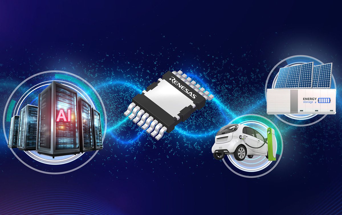
In a significant advancement for power electronics, Renesas, a global leader in semiconductor solutions, has officially announced the launch of what it describes as the industry’s first bidirectional 650 V-class Gallium Nitride (GaN) switch with integrated DC blocking capabilities. This innovative device is poised to streamline power conversion topologies, offering substantial benefits across diverse high-growth applications, including solar microinverters, advanced AI data centers, and crucial onboard EV chargers.
The introduction of the new Renesas GaN switch, designated as the TP65B110HRU, marks a pivotal moment in power semiconductor technology. Its design specifically targets the challenge of efficient bidirectional current management, a common requirement in many modern power systems. By blocking both positive and negative current within a single device, the TP65B110HRU eliminates the traditional reliance on more complex and component-heavy back-to-back FET (Field-Effect Transistor) arrangements, promising a new era of simplified and more robust power architectures.

Addressing Core Challenges in Power Conversion
Modern power conversion systems, particularly those operating at high voltages and demanding high efficiency, frequently grapple with the complexity and physical footprint associated with managing current flow in two directions. Conventional approaches often necessitate a configuration of two separate FETs connected in series, or ‘back-to-back,’ to achieve bidirectional blocking functionality. While effective, this method introduces inherent inefficiencies, increases component count, and demands more printed circuit board (PCB) area.
These traditional multi-component solutions contribute to higher system costs and can complicate thermal management. The integration of multiple discrete components also naturally leads to increased parasitic inductances and capacitances, which can negatively impact switching performance and overall system efficiency, especially at higher frequencies. Renesas’ new bidirectional 650V GaN switch directly addresses these long-standing issues by consolidating this functionality into a single, compact package.
Technical Prowess of the TP65B110HRU
The TP65B110HRU is engineered to offer superior performance and reliability. Technically, the device ingeniously combines a high-voltage bidirectional depletion-mode GaN die with two low-voltage silicon MOSFETs within a sophisticated co-packaged structure. This hybrid approach leverages the strengths of both GaN and silicon technologies to deliver optimal performance parameters crucial for demanding power applications.

The specifications of the Renesas GaN switch underscore its advanced capabilities. It supports a continuous AC/DC operation of ±650 V, demonstrating robust performance under typical operating conditions. Furthermore, it boasts an impressive ±800 V transient rating, providing an essential margin for handling momentary voltage spikes and ensuring system resilience. With a typical RSS,ON (on-state resistance) of 110 mΩ at 25 °C, the device minimizes conduction losses, thereby enhancing overall efficiency.
Critical to its performance is a 3 V typical threshold voltage, which ensures stable and predictable operation. The device also supports a maximum Vgs (gate-source voltage) of ±20 V and exhibits exceptional dv/dt immunity, exceeding 100 V/ns. This high immunity to rapid voltage changes across the device is vital for preventing false turn-on and ensuring stable operation in high-frequency switching environments.
Revolutionizing Solar Microinverters
The impact of this new Renesas GaN switch on solar power generation is particularly noteworthy. In the context of single-stage solar microinverters, which are critical for converting direct current (DC) from individual solar panels into alternating current (AC) for grid integration, the TP65B110HRU offers transformative advantages. Renesas states that deploying just two of these new bidirectional SuperGaN devices can effectively replace more complex multi-stage arrangements.
This reduction in complexity directly translates to halving the overall switch count within the microinverter design. Furthermore, it completely eliminates the need for intermediate DC-link capacitors, components that are often bulky, costly, and represent a common point of failure in power conversion systems. The tangible benefits are evident in real-world performance: a single-stage solar microinverter implementation using this technology has achieved an impressive efficiency exceeding 97.5%, demonstrating the significant gains in energy harvesting and reliability.
Advancing Onboard EV Chargers and AI Data Centers
Beyond solar applications, the Renesas GaN switch holds immense promise for the rapidly evolving electric vehicle (EV) market and the increasingly power-hungry infrastructure of AI data centers. For onboard EV chargers, the ability to achieve higher power density and reduce component count is paramount. Compact, efficient bidirectional power conversion is critical for both AC-DC conversion during charging and potentially for vehicle-to-grid (V2G) applications. The TP65B110HRU’s design facilitates smaller, lighter, and more efficient chargers, directly contributing to extending EV range and enhancing overall user experience.
Similarly, AI data centers are characterized by their insatiable demand for power and the need for extremely efficient power management to minimize operational costs and environmental impact. The significant energy consumption involved in training and running AI models necessitates highly optimized power delivery units and server power supplies. By simplifying topologies and boosting efficiency, the new Renesas GaN switch can lead to more compact and cooler-running power infrastructure within these data centers, reducing energy waste and improving system reliability.
Engineering Advantages: Depletion-Mode and Gate Drive Compatibility
The device’s physical form factor is also optimized for modern power applications. It comes in a top-side-cooled TOLT package, which is designed for efficient heat dissipation, a crucial factor in high-power systems. The industry-standard pinout of the package ensures ease of integration into existing designs and manufacturing processes.
A significant practical advantage highlighted by Renesas is the device’s compatibility with standard gate drivers, as it requires no negative gate drive. This feature differentiates it from many enhancement-mode bidirectional GaN devices, which can often demand more complicated and specialized gate-drive schemes, adding to system complexity and cost. The simplicity in driving the TP65B110HRU lowers the barrier to adoption and accelerates design cycles for engineers.
Rohan Samsi, Vice President of Renesas’s GaN Business Division, underscored the practical benefits of this innovation. He stated, “Customers can now achieve higher efficiency with fewer switching components, smaller PCB area and lower system cost.” This sentiment encapsulates the multi-faceted advantages that the new bidirectional 650V GaN switch brings to the power electronics landscape, promising not just technical superiority but also tangible economic benefits.
The Future of Power Electronics with Renesas GaN Technology
The introduction of this Renesas GaN switch signifies a pivotal step towards more efficient, compact, and cost-effective power conversion solutions. By addressing fundamental challenges in bidirectional current management and simplifying power topologies, Renesas is enabling advancements across critical sectors driving global technological progress.
As the demand for energy efficiency continues to grow in applications ranging from renewable energy systems to electric vehicles and the exponential expansion of AI infrastructure, innovations like the TP65B110HRU will be instrumental. This development not only enhances the performance of individual systems but also contributes to broader goals of energy conservation and sustainable technology deployment, solidifying Renesas’ position at the forefront of power semiconductor innovation.